
 EN
EN



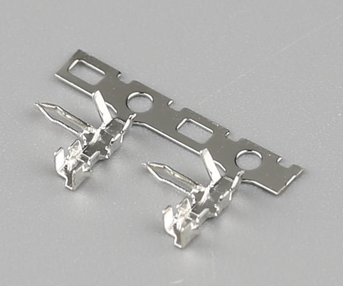
In the intricate architecture of modern electronic devices, the reliability of electrical connections determines operational stability, signal integrity, and overall system performance. Pin terminals serve as critical interface components that establish and maintain electrical pathways between circuit boards, connectors, and peripheral modules. Understanding how these seemingly simple components ensure secure contact reveals the sophisticated engineering principles underlying electronic assembly and the factors that separate functional connections from failure-prone designs. The mechanisms through which pin terminals achieve consistent electrical continuity involve precise material selection, geometric optimization, and mechanical design strategies that accommodate manufacturing tolerances while resisting environmental stresses throughout the device lifecycle.
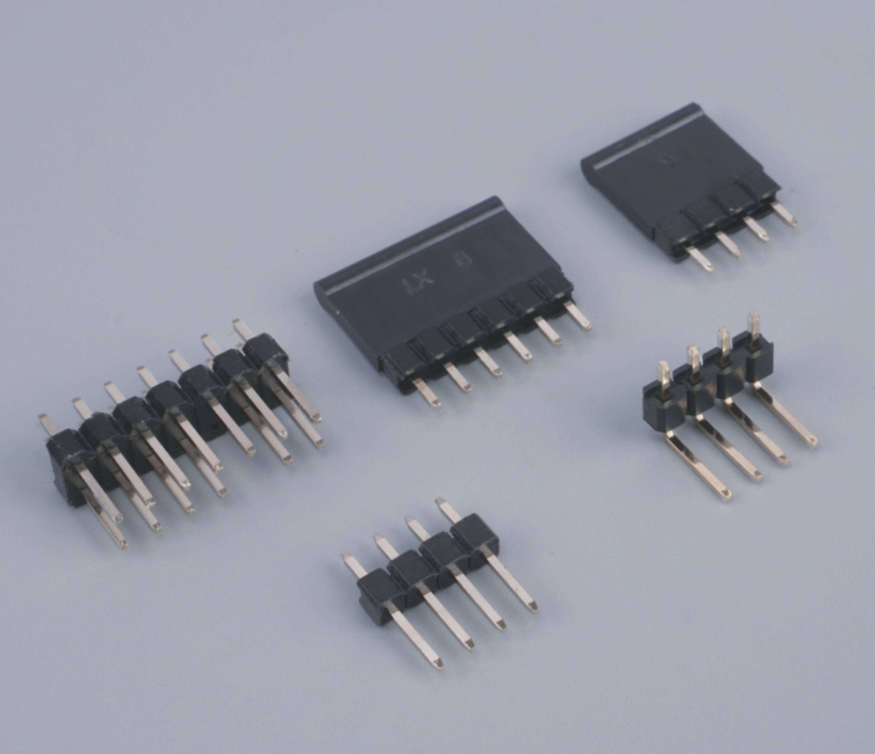
The challenge of maintaining secure contact extends beyond initial assembly, encompassing thermal cycling effects, vibration resistance, oxidation prevention, and contact force degradation over time. Engineers must balance competing requirements including insertion force during assembly, contact resistance during operation, retention force against separation, and the need for field serviceability in certain applications. This comprehensive exploration examines the physical principles, design features, material characteristics, and application-specific considerations that enable pin terminals to function as dependable electrical interfaces across diverse electronic systems from consumer products to industrial control equipment and telecommunications infrastructure.
Mechanical Design Principles Behind Contact Security
Contact Force Generation Through Elastic Deformation
The fundamental mechanism by which pin terminals establish secure electrical contact relies on controlled elastic deformation of conductive elements. When a pin terminal engages with its mating receptacle or socket, the geometry of the contact interface creates an interference fit that generates normal force perpendicular to the contact surfaces. This contact force maintains physical pressure between conductive materials, breaking through microscopic surface oxidation and establishing multiple metallic contact points that enable current flow. The magnitude of this force must exceed minimum thresholds to ensure stable electrical performance while remaining below levels that would cause permanent plastic deformation or insertion difficulties during assembly.
Engineers design pin terminals with specific spring characteristics that determine the force-displacement relationship during mating. Cantilever beam sections, formed contact zones, and strategically placed flexure points create predictable elastic behavior that accommodates dimensional variations in both the pin terminal and its mating component. The elastic modulus of the base material, combined with the geometric moment of inertia of the contact spring section, determines how much force develops for a given deflection distance. This relationship must account for tolerance stackups in manufacturing, thermal expansion differentials, and the settling effects that occur as contact surfaces conform microscopically over the initial connection period.
Retention Mechanisms and Separation Resistance
Beyond establishing initial contact, pin terminals incorporate design features that resist accidental disconnection under mechanical stress conditions encountered during device operation. Retention barbs, locking tabs, and interference features engage with housing geometries or mating connector bodies to create mechanical resistance against axial separation forces. These retention mechanisms function independently from the electrical contact force system, providing redundant security that prevents connection loss even if contact spring forces degrade over time. The separation force required to overcome these retention features typically ranges from several newtons to tens of newtons depending on application requirements and the need for field serviceability.
The effectiveness of retention systems depends on the interaction between pin terminal features and the surrounding dielectric housing material. Thermoplastic materials commonly used in connector housings exhibit viscoelastic behavior that can allow retention features to relax under sustained load or elevated temperature conditions. Designers must therefore specify retention geometries with sufficient engagement depth and feature strength to maintain functionality across the anticipated temperature range and mechanical loading scenarios. Some advanced pin terminals incorporate multiple retention zones along their length, distributing separation resistance and reducing stress concentration on individual features that might otherwise fail under shock or vibration conditions.
Geometric Optimization for Contact Stability
The dimensional characteristics of pin terminals directly influence contact reliability through their effect on current density distribution, thermal management, and mechanical alignment. Contact geometry determines the effective contact area where electrical current transfers between mating components, with concentrated contact points creating higher current density that can lead to localized heating and accelerated degradation. Pin terminals designed for higher current applications incorporate wider contact surfaces or multiple contact points that distribute current flow and reduce power dissipation at the interface. The balance between contact area and contact force becomes critical, as excessive area with insufficient pressure results in poor electrical performance despite apparent mechanical engagement.
Cross-sectional profiles of pin terminals vary significantly based on application requirements, with square, rectangular, and circular geometries each offering distinct advantages. Square pin terminals provide four potential contact edges that can accommodate angular misalignment between mating components while maintaining at least two-point contact. Circular pins offer uniform contact characteristics regardless of rotational orientation and simplified insertion dynamics, making them preferred for high-reliability applications requiring repeated mating cycles. The dimensional precision of these profiles directly impacts contact consistency, with tighter manufacturing tolerances enabling more predictable contact force and electrical performance across production volumes.
Material Selection and Surface Engineering
Base Material Properties for Mechanical Performance
The substrate material from which pin terminals are formed determines their fundamental mechanical characteristics including elastic modulus, yield strength, fatigue resistance, and formability. Copper alloys dominate pin terminal manufacturing due to their combination of electrical conductivity, mechanical workability, and cost-effectiveness. Phosphor bronze alloys provide excellent spring properties with high fatigue resistance, making them suitable for contact elements that must maintain force through millions of insertion cycles. Beryllium copper offers superior strength and conductivity but raises material cost and processing complexity. Brass alloys serve cost-sensitive applications where moderate electrical performance suffices and high-cycle durability is not required.
The temper condition or work-hardening state of the base material critically affects contact performance characteristics. Pin terminals manufactured from fully annealed material exhibit excessive compliance that allows contact forces to decay rapidly under mechanical stress. Conversely, materials in excessively hardened states may fracture during forming operations or exhibit brittle failure modes under shock loading. Manufacturers typically specify half-hard or spring-temper conditions that balance formability during stamping operations with the mechanical resilience required for reliable contact performance. The grain structure resulting from cold working processes influences long-term stress relaxation behavior, with finer grain structures generally providing better dimensional stability over thermal cycling exposure.
Plating Systems for Contact Resistance and Durability
Surface finish engineering constitutes a critical aspect of pin terminal design, as the outermost molecular layers determine contact resistance, corrosion protection, and tribological behavior during insertion and withdrawal cycles. Noble metal platings including gold and its alloys provide the lowest and most stable contact resistance due to their immunity to oxidation and sulfidation reactions that create insulating films on base metals. Gold plating thickness typically ranges from 0.76 to 2.54 micrometers for electronics applications, with thicker deposits providing extended durability in high-cycle connector applications. Nickel underplating beneath gold layers prevents copper diffusion that would otherwise compromise contact performance over time at elevated operating temperatures.
Cost considerations drive the adoption of alternative plating systems for applications tolerating higher contact resistance or limited environmental exposure. Tin and tin-alloy platings offer economical protection for pin terminals in benign environments, though the formation of tin oxide films and the potential for whisker growth require careful process control and application assessment. Silver plating provides excellent conductivity and remains more affordable than gold, but tarnishing from atmospheric sulfur compounds limits its suitability to controlled environments or sealed connector systems. Some specialized pin terminals incorporate selective plating strategies where noble metals protect high-stress contact zones while more economical finishes cover structural sections that do not participate in electrical conduction.
Surface Texture and Microstructure Effects
The microscopic topography of pin terminal contact surfaces influences real contact area and the effectiveness of mechanical forces in establishing electrical pathways. Even apparently smooth metallic surfaces exhibit roughness at micrometer and nanometer scales, with current flow concentrating at asperity peaks where metals achieve intimate contact. The relationship between apparent contact area and real contact area depends on surface roughness characteristics, contact force magnitude, and the plastic deformation behavior of surface asperities under compressive stress. Pin terminals with excessively rough surfaces require higher contact forces to achieve adequate real contact area, while surfaces that are too smooth may exhibit poor tribological behavior during insertion with increased tendency for galling or cold welding.
Plating process parameters directly control surface finish characteristics, with factors including current density, bath chemistry, and post-plating treatments affecting both roughness and grain structure. Bright tin platings produced through organic additives exhibit finer grain structures than matte tin finishes, influencing whisker formation propensity and contact resistance stability. Gold platings can be deposited in soft or hard tempers with distinct tribological properties affecting wear resistance during repeated mating cycles. The interaction between base material roughness and plating thickness creates complex surface engineering scenarios where underlying substrate texture may telegraph through thin plating layers, necessitating careful process specification to achieve desired contact performance characteristics.
Environmental Resistance and Long-Term Stability
Oxidation Prevention and Corrosion Protection
The ongoing challenge of maintaining low contact resistance throughout device operational life requires pin terminals to resist oxidation and corrosion processes that create insulating barriers at electrical interfaces. Base metals including copper and its alloys readily form oxide layers when exposed to atmospheric oxygen, with cuprous and cupric oxides exhibiting electrical resistivity several orders of magnitude higher than metallic copper. While contact force can mechanically disrupt thin oxide films during initial mating, ongoing oxidation during service creates progressive resistance increases that eventually compromise signal integrity or power delivery capability. This degradation mechanism becomes particularly severe in elevated temperature applications where oxidation kinetics accelerate exponentially with thermal energy.
Protective plating systems function as sacrificial barriers that isolate reactive base metals from corrosive atmospheric constituents. The effectiveness of this protection depends on plating integrity, with pores or defects creating galvanic cells that can accelerate localized corrosion of underlying substrate material. Pin terminals designed for harsh environment deployment incorporate thicker noble metal platings or employ barrier layer strategies where multiple plating layers provide redundant protection against corrosion pathways. Some applications specify sealed connector systems with elastomeric seals that exclude moisture and corrosive gases, enabling the use of more economical plating systems that would otherwise prove inadequate in open environmental exposure.
Thermal Cycling and Stress Relaxation Phenomena
Electronic devices experience temperature fluctuations during operation and across seasonal ambient variations, subjecting pin terminals to thermal expansion and contraction cycles that affect contact force maintenance. Differential thermal expansion between dissimilar materials in connector assemblies creates mechanical stresses at pin terminal interfaces, with expansion coefficient mismatches potentially causing either excessive stress during heating or contact force loss during cooling phases. The magnitude of these effects scales with temperature range, component dimensions, and the constraint conditions imposed by housing geometries and circuit board mounting arrangements.
Prolonged exposure to elevated temperatures induces stress relaxation in the spring elements of pin terminals, causing gradual reduction in contact force even without mechanical disturbance. This time-temperature dependent phenomenon results from thermally activated dislocation motion within the crystal structure of contact spring materials, allowing internal stresses to dissipate through creep deformation. The rate of stress relaxation depends strongly on temperature, with each 10-degree Celsius increase typically doubling the relaxation rate. Engineers must therefore derate contact force specifications for elevated temperature applications or specify enhanced alloys with superior creep resistance. Some advanced pin terminals incorporate design features that compensate for stress relaxation by establishing initial contact forces substantially above minimum functional requirements, ensuring adequate performance despite predictable force decay over the design life.
Vibration Resistance and Fretting Corrosion Prevention
Applications involving mechanical vibration or shock loading present distinct challenges for pin terminal contact security, as oscillatory relative motion between contact surfaces can disrupt electrical pathways and generate progressive wear. Fretting corrosion represents a particularly insidious degradation mechanism where microscopic sliding motion between nominally stationary contacts breaks protective oxide films and exposes fresh metal that rapidly re-oxidizes, creating an accumulation of wear debris that increases contact resistance. The amplitude of relative motion required to initiate fretting may be only a few micrometers, making this phenomenon relevant even in applications without obvious vibratory loading.
Pin terminals combat fretting through design strategies that maximize normal force at contact interfaces, thereby increasing the friction force required to initiate relative motion. Contact geometries with larger engagement depths and multiple contact points distribute vibrational energy and reduce the likelihood of simultaneous motion at all contact locations. Material selection also influences fretting resistance, with harder contact surfaces and noble metal platings exhibiting superior performance compared to soft base metals. Some specialized applications employ pin terminals with mechanical locking features that positively constrain relative motion independent of friction forces, providing absolute fretting prevention in severe vibration environments such as automotive underhood electronics or aerospace applications.
Application-Specific Design Considerations
Current Rating and Power Handling Capacity
The maximum current that pin terminals can reliably conduct depends on the combined effects of resistive heating, thermal dissipation paths, and temperature rating of surrounding materials. Current flow through the bulk conductor and contact interface generates heat proportional to the square of current magnitude and the total resistance of the current path. This power dissipation must remain within limits that prevent excessive temperature rise, which could damage plating systems, degrade plastic housing materials, or accelerate stress relaxation in contact springs. The thermal resistance between the pin terminal and ambient environment determines the steady-state temperature rise for a given power dissipation level, with factors including air circulation, contact with heat-sinking structures, and thermal conductivity of housing materials all influencing heat removal effectiveness.
Engineers calculate pin terminal current ratings by establishing temperature rise limits typically ranging from 30 to 50 degrees Celsius above ambient, then working backward through thermal and electrical resistance values to determine the corresponding current level. The cross-sectional area of the conductor sets bulk resistance, while contact interface design determines contact resistance contribution. High-current pin terminals incorporate enlarged conductor cross-sections and optimized contact geometries that minimize total resistance, thereby reducing power dissipation for a given current level. Some designs employ multiple parallel contact points that both distribute current flow and provide redundancy against single-point contact degradation, improving reliability in critical power delivery applications.
Signal Integrity Requirements for High-Speed Applications
Modern electronic systems increasingly demand pin terminals capable of maintaining signal integrity for high-frequency digital communications and high-bandwidth analog signals. At frequencies above several hundred megahertz, conventional low-frequency electrical behavior gives way to transmission line effects where impedance control, signal reflection management, and crosstalk minimization become paramount. Pin terminals designed for these applications require careful attention to geometric parameters that determine characteristic impedance, including conductor dimensions, dielectric spacing, and the proximity of adjacent signal paths. Impedance discontinuities at pin terminal interfaces create signal reflections that degrade signal quality, making controlled-impedance design essential for gigabit-per-second data rates.
The electrical length of pin terminals relative to signal wavelength determines whether they function as simple connections or as transmission line elements requiring impedance matching. At frequencies where pin terminal length exceeds approximately one-tenth of signal wavelength, transmission line behavior dominates and careful impedance design becomes necessary. For differential signaling applications common in high-speed serial communications, pin terminals must maintain tight coupling between signal pairs to preserve common-mode rejection and minimize mode conversion. Some advanced pin terminal designs incorporate ground pins positioned to provide electromagnetic shielding between adjacent signal paths, reducing crosstalk in dense connector configurations where multiple high-speed channels operate in close proximity.
Miniaturization Constraints and Density Optimization
The persistent trend toward smaller, more compact electronic devices drives demand for pin terminals with reduced pitch dimensions and minimized footprint requirements. However, physical scaling presents fundamental challenges as contact force requirements do not decrease proportionally with size reduction. Smaller pin terminals incorporate thinner conductor cross-sections that increase electrical resistance and reduce current capacity while simultaneously requiring sufficient material volume to generate adequate contact spring forces. The relationship between these competing requirements creates practical limits to miniaturization, with pin terminal pitch dimensions rarely dropping below 0.4 millimeters for manual assembly applications due to handling and inspection constraints.
High-density pin terminal arrays require careful attention to electromagnetic coupling between adjacent contacts, as reduced spacing increases capacitive and inductive crosstalk that can compromise signal quality in sensitive analog or high-speed digital applications. Designers employ various strategies to mitigate these effects including ground pin allocation, signal pair arrangement optimization, and the use of plastic housing materials with low dielectric constants that reduce parasitic capacitance. Manufacturing process capabilities ultimately limit achievable pin terminal density, with stamping die complexity, plating thickness uniformity, and assembly precision all degrading as feature sizes decrease. Some applications requiring extreme density employ alternative interconnection technologies including ball grid arrays or land grid arrays where pin terminals give way to fundamentally different contact mechanisms more amenable to very fine pitch implementation.
FAQ
What is the typical lifespan of pin terminals in terms of mating cycles?
Pin terminal durability depends heavily on design specifics, material selection, and operating conditions, but commercial-grade contacts typically withstand 50 to 500 mating cycles before contact resistance increases beyond acceptable limits. Gold-plated pin terminals with optimized spring geometries can achieve 1,000 to 10,000 cycles in benign environments, while specialized high-cycle designs for telecommunications and test equipment applications may reach 100,000 cycles or more. Tin-plated alternatives generally exhibit shorter lifespans due to wear-through of plating and oxide film formation. Operating environment factors including temperature extremes, vibration exposure, and atmospheric contamination can significantly reduce practical service life below theoretical cycle ratings.
How does contact resistance affect overall system performance?
Contact resistance at pin terminal interfaces contributes directly to voltage drop in power distribution paths and signal attenuation in communication circuits. For power delivery applications, excessive contact resistance generates heat that wastes energy and may trigger thermal protection mechanisms or damage temperature-sensitive components. In sensitive analog circuits, contact resistance variations introduce noise and measurement errors that degrade system accuracy. High-speed digital systems experience signal reflections and impedance mismatches from resistive discontinuities at pin terminal interfaces, potentially causing bit errors or limiting maximum data rates. Well-designed pin terminals maintain contact resistance below 10 milliohms for power applications and often below 2 milliohms for signal paths, ensuring negligible impact on overall system electrical performance.
Can pin terminals be successfully reused after disconnection?
The viability of reusing pin terminals after disconnection depends on the contact design, plating system, and the care exercised during separation. Gold-plated pin terminals generally tolerate multiple reconnection cycles because noble metal surfaces resist oxidation and wear, maintaining low contact resistance through several disconnection and reinsertion events. Tin-plated alternatives fare less well, as each mating cycle abrades the plating and exposes underlying base metal that oxidizes, progressively increasing contact resistance with repeated use. Physical damage during removal processes including bending, stretching, or scoring of contact surfaces permanently compromises performance. Professional service procedures minimize such damage through controlled extraction forces and proper tooling, but field repairs involving pin terminal reuse should include contact resistance verification to ensure continued reliability.
What environmental factors most severely impact pin terminal reliability?
Humidity combined with atmospheric pollutants creates the most aggressive environment for pin terminal degradation, as moisture enables electrochemical corrosion processes while sulfur compounds, chlorides, and industrial contaminants accelerate oxidation and form insulating films on contact surfaces. Elevated temperature exacerbates these effects by increasing reaction kinetics and inducing stress relaxation that reduces contact force over time. Thermal cycling generates mechanical fatigue in spring elements while differential thermal expansion creates interface stresses that may disrupt electrical pathways. Vibration and mechanical shock cause fretting corrosion and potential physical separation of mated contacts. Applications in marine, industrial, or automotive environments typically require sealed connector systems with enhanced plating specifications or conformal coating protection to achieve reliability targets comparable to benign office or residential conditions.

