


Modern electronics manufacturing faces mounting pressure to deliver devices that are smaller, more reliable, and capable of operating in increasingly demanding environments. Engineers confront a cascade of design obstacles: space constraints that demand ultra-compact interconnection solutions, reliability requirements that leave no room for connection failures, and assembly processes that must balance speed with precision. These challenges converge at a critical component often overlooked in system design—the connector. Among the solutions that have emerged to address these specific pain points, JST connectors have become instrumental in resolving interconnection challenges across consumer electronics, automotive systems, industrial equipment, and medical devices. This article examines the precise technical and operational problems that JST connectors solve, explaining why design engineers increasingly specify these components when conventional connector solutions fall short.
The proliferation of portable electronics, IoT devices, and miniaturized industrial controls has created a fundamental conflict between physical space availability and functional requirements. As circuit boards shrink and component density increases, traditional connector technologies struggle to maintain adequate contact reliability while fitting into reduced footprints. Simultaneously, manufacturing environments demand connection systems that support automated assembly without compromising mechanical integrity or electrical performance. JST connectors address these converging pressures through deliberate design features that balance miniaturization with durability, automation compatibility with manual serviceability, and cost efficiency with performance reliability. Understanding the specific challenges these connectors solve provides essential context for engineers making critical design decisions in space-constrained, reliability-critical applications.
Space Constraints and Miniaturization Challenges in High-Density Designs
The Physical Footprint Problem in Compact Electronics
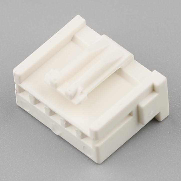
Contemporary electronic devices operate under relentless pressure to reduce physical dimensions while expanding functionality. Smartphones, wearable devices, drone controllers, and compact medical instruments exemplify products where every cubic millimeter carries design significance. Traditional connector systems with large housings, extended mating profiles, and substantial PCB footprints create bottlenecks in achieving target size specifications. JST connectors directly address this challenge through miniaturized contact geometries and low-profile housing designs that occupy minimal board real estate. These connectors utilize fine-pitch contact arrangements, typically ranging from 1.0mm to 2.5mm pitch configurations, enabling multiple signal and power connections within extremely confined spaces. The reduced height profiles, often below 3mm for complete mated assemblies, allow designers to position components on both sides of circuit boards without interference, maximizing usable PCB area in three-dimensional space-constrained environments.
Maintaining Contact Reliability Despite Reduced Dimensions
Miniaturization introduces a fundamental engineering challenge: as connector dimensions decrease, maintaining adequate contact force and electrical stability becomes increasingly difficult. Smaller contacts have reduced contact areas, making them more susceptible to oxidation, contamination, and mechanical degradation. JST connectors solve this problem through precision-engineered contact designs that optimize spring force distribution across reduced contact surfaces. The contacts employ carefully calculated beam geometries and material selections—typically phosphor bronze or beryllium copper alloys with gold or tin plating—that maintain reliable electrical continuity despite their diminutive size. This design approach ensures that even connectors with sub-millimeter contact pitches deliver stable contact resistance over thousands of mating cycles. Engineers benefit from connector solutions that meet space requirements without sacrificing the electrical performance standards necessary for signal integrity in high-speed data transmission or stable power delivery in battery-operated devices.
Managing Wire-to-Board Connections in Restricted Spaces
Space limitations extend beyond the connector body itself to include wire routing and strain relief considerations. In compact assemblies, cable harnesses must navigate tight bend radii and limited clearance zones without compromising electrical performance or mechanical durability. JST connectors incorporate right-angle and vertical wire entry configurations that optimize cable routing options in confined enclosures. The connector housings feature integrated strain relief structures that protect wire terminations from mechanical stress without requiring additional external components that would consume valuable space. This design integration proves particularly valuable in battery compartments, sensor modules, and internal subsystem interconnections where cable management directly impacts assembly feasibility. By providing multiple wire exit orientations and compact strain relief within the connector footprint, JST connectors enable designers to achieve clean, organized wire routing even in severely space-constrained applications where traditional connectors would create assembly conflicts or require larger enclosure volumes.
Manufacturing Efficiency and Assembly Process Challenges
Automated Pick-and-Place Compatibility
Modern electronics manufacturing relies heavily on automated assembly processes to achieve the production volumes and cost structures market demands require. Connectors that cannot accommodate automated placement create bottlenecks that force expensive manual intervention or specialized handling equipment. JST connectors solve this challenge through standardized packaging formats and housing geometries optimized for automated pick-and-place equipment. The connectors ship in tape-and-reel packaging with precise pocket dimensions and spacing that match industry-standard automated assembly systems. Housing designs incorporate features such as vacuum pick-up surfaces, alignment references, and consistent geometric profiles that enable reliable robotic handling without position errors or orientation mistakes. This automation compatibility extends to the PCB mounting process, where JST connectors utilize through-hole and surface-mount termination styles with standardized footprints that integrate seamlessly with existing PCB design libraries and assembly equipment. Manufacturers benefit from reduced labor costs, improved placement accuracy, and higher throughput rates compared to connector systems requiring manual handling or custom automation fixtures.
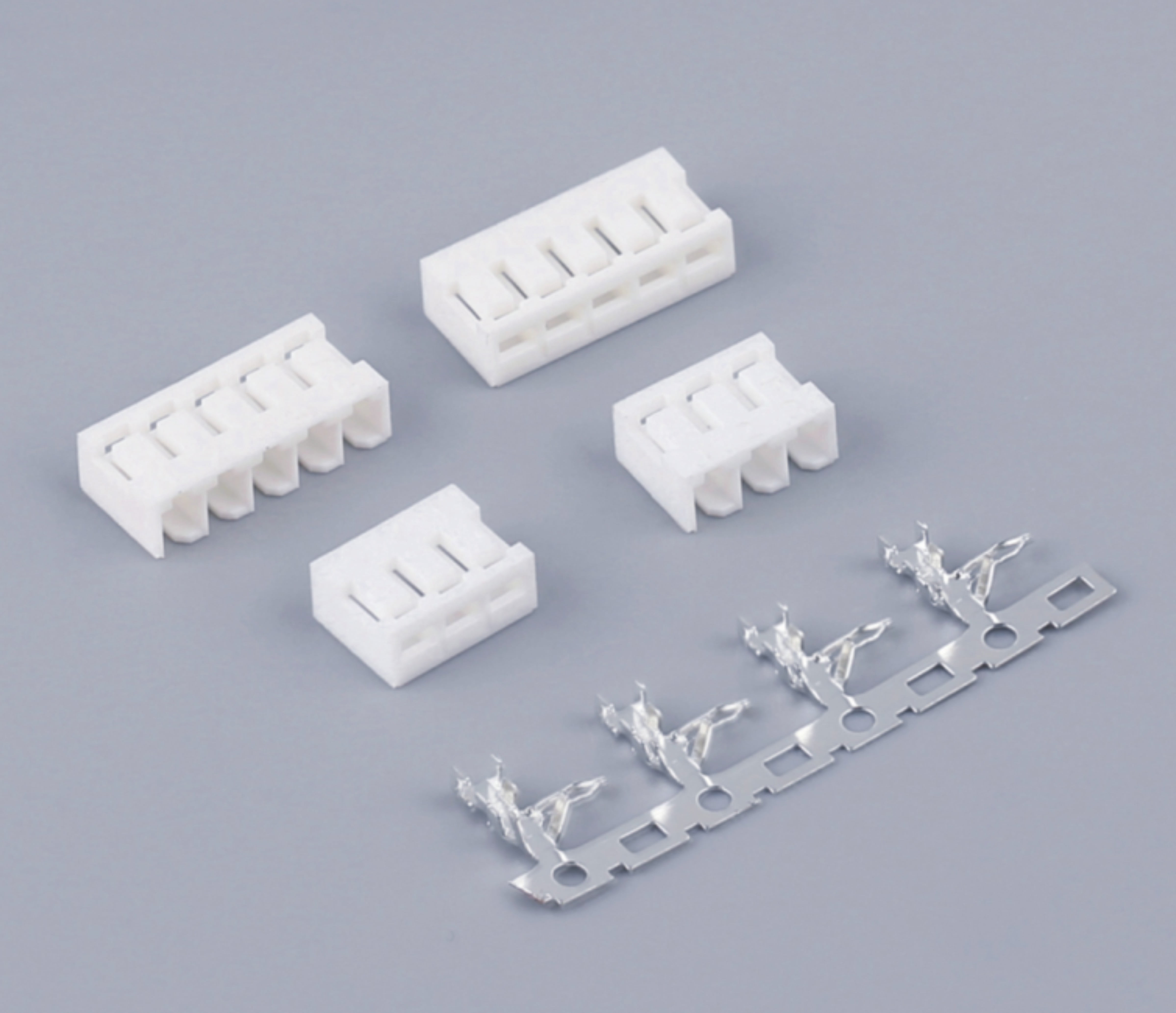
Simplifying Wire Harness Assembly and Crimping Operations
Wire harness assembly represents a significant portion of total connector implementation costs, particularly in products requiring multiple interconnection points or custom cable lengths. Complex crimping procedures, difficult contact insertion processes, and high rates of assembly errors drive up manufacturing costs and extend production timelines. JST connectors address these challenges through standardized crimping specifications and connector housing designs that facilitate rapid, error-resistant contact insertion. The crimp terminals feature clearly defined inspection windows that allow quality verification without specialized equipment, reducing scrap rates and rework requirements. Housing designs incorporate positive locking mechanisms that provide tactile and audible feedback when contacts seat properly, enabling assembly operators to confirm correct insertion without additional testing steps. Pre-assembled cable options further streamline manufacturing by providing ready-to-install harnesses with factory-crimped terminations that meet consistent quality standards. These features collectively reduce harness assembly time, minimize training requirements for assembly personnel, and improve first-pass yield rates in production environments where labor efficiency directly impacts product cost structures.
Reducing Quality Control and Inspection Requirements
Quality assurance processes consume significant time and resources in electronics manufacturing, particularly when connector failures can cause field returns or safety incidents. Connectors that require extensive electrical testing, mechanical inspection, or specialized quality verification equipment add costs without adding value to the end product. JST connectors incorporate design features that inherently reduce quality control requirements through self-verifying assembly characteristics and robust construction that minimizes defect opportunities. The positive locking mechanisms and color-coded housings enable visual inspection protocols that quickly identify assembly errors without electrical testing. Standardized contact retention specifications ensure that properly assembled connectors maintain mechanical integrity throughout their service life, reducing the need for pull-force testing or other mechanical validation procedures. Housing materials and contact plating systems meet established reliability standards, allowing manufacturers to implement sampling-based inspection protocols rather than 100% testing requirements. This reduction in quality control overhead translates directly to lower manufacturing costs and shorter production cycle times while maintaining the reliability standards critical for customer satisfaction and warranty cost control.
Mechanical Reliability and Vibration Resistance Issues
Addressing Intermittent Connection Failures in Dynamic Environments
Electronic systems operating in automotive, industrial, and aerospace applications experience continuous vibration, shock, and mechanical stress that can compromise connector reliability. Intermittent connection failures caused by vibration-induced contact separation represent one of the most difficult failure modes to diagnose and remedy in field-deployed equipment. Traditional friction-fit connectors often lack sufficient contact retention force to maintain stable connections under sustained vibration exposure. JST connectors solve this challenge through positive locking mechanisms that mechanically secure mated connector halves beyond simple friction retention. Latch designs incorporate spring-loaded tabs, ramp-and-detent features, or threaded locking collars that require deliberate action to disconnect, preventing inadvertent separation under vibration or shock loading. Contact designs utilize increased spring force and longer engagement lengths that maintain electrical continuity even when housing components experience minor displacement. These mechanical design features prove essential in automotive electronics, industrial control panels, and portable equipment where connection reliability directly affects system functionality and user safety under real-world operating conditions.
Managing Contact Fretting and Wear in High-Cycle Applications
Applications requiring frequent connector mating and unmating cycles face accelerated contact degradation through fretting wear—microscopic relative motion between contact surfaces that removes protective platings and creates insulating oxide layers. This phenomenon becomes particularly problematic in maintenance-accessible equipment, test fixtures, and reconfigurable systems where connectors may undergo hundreds or thousands of mating cycles over their service life. JST connectors address fretting wear through contact geometry designs that maximize wiping action during mating cycles, mechanically disrupting oxide formation and maintaining low contact resistance despite repeated connections. Material selections emphasize hard gold plating over contact engagement areas in applications requiring extended cycle life, providing superior wear resistance compared to tin or other economical plating options. Spring designs maintain consistent contact force throughout the connector's rated mating cycle life, compensating for minor material fatigue or dimensional changes that occur with repeated use. Engineers specifying JST connectors for high-cycle applications benefit from published mating cycle ratings that reflect realistic use conditions, enabling confident connector selection for maintenance panels, diagnostic ports, and other frequently accessed connection points.
Preventing Contact Corrosion in Harsh Environmental Conditions
Electronic systems deployed in outdoor environments, marine applications, or industrial settings face exposure to humidity, temperature extremes, chemical contaminants, and corrosive atmospheres that accelerate connector degradation. Contact corrosion creates increased resistance, voltage drops, and eventual connection failure that compromises system reliability. Standard connector designs often lack adequate environmental sealing or use contact materials vulnerable to corrosion in aggressive environments. JST connectors solve these challenges through housing designs that incorporate environmental sealing features and contact plating systems selected for corrosion resistance in specific operating environments. Sealed housing variants utilize elastomeric gaskets and positive sealing interfaces that meet IP67 or higher ingress protection ratings, preventing moisture and contaminant entry at the mating interface. Contact plating options include hard gold for maximum corrosion resistance, selective gold plating for cost-optimized performance, or specialized tin-lead alloys for applications requiring solderable terminations with enhanced oxidation resistance. The combination of mechanical sealing and appropriate surface treatments extends connector service life in challenging environments where conventional connectors would require frequent replacement or protective measures that increase system cost and complexity.
Electrical Performance Optimization in Signal-Critical Applications
Maintaining Signal Integrity in High-Speed Data Transmission
Modern electronics increasingly rely on high-speed digital communication protocols that demand controlled impedance, minimal crosstalk, and stable electrical characteristics throughout the signal path. Connectors represent potential discontinuities in transmission lines where impedance mismatches, increased capacitance, or inadequate shielding can degrade signal quality and limit achievable data rates. JST connectors designed for signal-critical applications address these challenges through controlled contact geometries and housing configurations that minimize electrical discontinuities. Contact spacing and ground pin placement follow careful electromagnetic design principles that reduce crosstalk between adjacent signal pairs, maintaining signal integrity in differential signaling applications. Low insertion loss characteristics preserve signal amplitude in high-frequency applications where connector attenuation would otherwise limit transmission distances or require signal conditioning circuitry. Shielded variants incorporate 360-degree EMI shielding that maintains consistent shield termination and prevents electromagnetic interference from coupling into sensitive signal paths. These electrical design features enable JST connectors to support modern communication protocols including USB, HDMI, and proprietary high-speed serial interfaces that would suffer unacceptable performance degradation with electrically unoptimized connector designs.
Achieving Stable Power Delivery in High-Current Applications
Battery-powered devices and power distribution systems require connector solutions that deliver stable voltage under varying load conditions while managing thermal dissipation from current flow through contact interfaces. Inadequate contact area, high contact resistance, or poor current distribution across multiple contacts creates voltage drops that reduce available power to downstream circuits and generates heat that can damage connector components or adjacent assemblies. JST connectors designed for power applications solve these challenges through increased contact cross-sections, multiple parallel contacts for high-current paths, and contact materials optimized for low bulk resistivity. Power pin configurations utilize wider contacts or multiple redundant contacts that distribute current flow and reduce per-contact current density, minimizing resistive heating and improving thermal stability. Contact spring designs maintain high contact force that reduces interface resistance and improves current-carrying capacity within the connector's temperature rating. Current rating specifications reflect realistic operating conditions including ambient temperature, current distribution, and mating cycle history, enabling engineers to confidently specify connectors that will maintain stable power delivery throughout their service life. This attention to power delivery performance proves particularly valuable in battery management systems, motor control applications, and LED lighting systems where connector voltage drop directly impacts system efficiency and operational reliability.
Eliminating Ground Bounce and Power Distribution Noise
Digital circuits with fast switching transitions generate transient currents that flow through ground and power distribution networks, creating voltage fluctuations known as ground bounce and power supply noise. Connectors with inadequate ground pin count, poor pin arrangement, or high inductance in power and ground paths exacerbate these problems, potentially causing logic errors or analog circuit performance degradation. JST connectors address power integrity challenges through pin assignment strategies that interleave power and ground contacts with signal pins, reducing inductance in the power distribution path and providing local return current paths that minimize ground bounce. Increased ground pin count in high-speed digital applications provides multiple low-impedance return paths that distribute transient currents and reduce voltage fluctuations at the connector interface. Contact designs minimize lead inductance through short, wide conductor geometries that reduce the impedance seen by high-frequency transient currents. These electrical design considerations prove essential in mixed-signal systems, high-speed digital designs, and applications where power supply integrity directly affects analog measurement accuracy or communication link stability, enabling JST connectors to support demanding electrical performance requirements without compromising the space efficiency and mechanical reliability that drive initial connector selection.
Cost Optimization and Supply Chain Management Concerns
Balancing Performance Requirements with Budget Constraints
Product development teams face constant pressure to minimize bill-of-material costs while maintaining performance and reliability standards that meet customer expectations and competitive requirements. Over-specified connectors waste resources on unnecessary capabilities, while under-specified components create field failures and warranty costs that far exceed initial savings. JST connectors solve this optimization challenge through broad product families that span multiple performance and price points, enabling precise matching between application requirements and connector capabilities. Standard product lines provide cost-effective solutions for general-purpose applications where premium features would provide no functional benefit. Enhanced variants offer sealed housings, extended temperature ratings, or increased cycle life specifications for demanding applications that justify incremental cost increases. This product family architecture allows engineers to specify exactly the performance level required without paying for unnecessary capabilities or accepting inadequate specifications. The availability of both wire-to-board and wire-to-wire configurations within compatible product families further optimizes system cost by enabling standardized inventory and tooling investments across multiple connection types, reducing the total cost of connector implementation beyond the simple per-unit component price.
Ensuring Global Availability and Supply Chain Stability
Electronics manufacturers increasingly operate global supply chains with production facilities, contract manufacturers, and distribution channels spanning multiple continents. Connector selections that lack worldwide availability or depend on single-source suppliers create supply chain vulnerabilities that can halt production lines and delay product launches. JST connectors address these concerns through extensive global distribution networks and manufacturing capacity that ensures consistent availability across major electronics manufacturing regions. The standardized nature of JST connector specifications enables multiple authorized distributors to stock common configurations, reducing lead times and enabling responsive supply chain management. Compatible contact systems and housing families allow designers to source components from multiple geographical locations while maintaining interchangeability and consistent performance characteristics. This supply chain robustness proves particularly valuable during component shortages or supply disruptions where single-source components may become unavailable for extended periods, potentially forcing expensive redesigns or production delays that impact time-to-market objectives and revenue recognition timelines.
Reducing Long-Term Maintenance and Lifecycle Costs
The true cost of connector implementation extends far beyond initial purchase price to include field service expenses, warranty claims, and maintenance labor throughout product lifecycle. Connectors prone to wear, environmental degradation, or assembly errors generate ongoing costs that accumulate over years of product service life. JST connectors minimize lifecycle costs through robust mechanical designs that maintain performance throughout rated specifications, reducing premature failure rates and associated warranty expenses. The widespread adoption of JST connector standards ensures that replacement parts remain available for extended periods, supporting field service operations and maintenance programs without forcing premature equipment retirement due to connector obsolescence. Standardized contact crimping and housing assembly procedures reduce training costs for service personnel and minimize the specialized tooling required for field repairs or upgrades. These lifecycle cost advantages prove particularly significant in industrial equipment, automotive applications, and durable goods where field service costs substantially impact total cost of ownership and influence purchasing decisions, making connector reliability and serviceability important competitive differentiators beyond initial product price considerations.
FAQ
What specific size advantages do JST connectors provide compared to traditional connector types?
JST connectors offer significant miniaturization advantages through fine-pitch contact arrangements typically ranging from 1.0mm to 2.5mm spacing, compared to 2.54mm or larger pitches common in traditional connectors. Housing heights often measure below 3mm for complete mated assemblies, enabling dual-sided component placement on compact circuit boards. The reduced footprint allows designers to achieve 30-50% space savings compared to conventional connector systems while maintaining equivalent electrical and mechanical performance specifications. This miniaturization proves essential in portable electronics, wearable devices, and high-density industrial controls where board space directly limits feature implementation or determines final product dimensions.
How do JST connectors maintain reliability in high-vibration automotive and industrial environments?
JST connectors designed for dynamic environments incorporate positive locking mechanisms including spring-loaded latches, ramp-and-detent retention features, and mechanical locks that prevent vibration-induced disconnection. Contact designs utilize increased spring force specifications and extended engagement lengths that maintain electrical continuity despite minor housing displacement under shock or vibration loading. Material selections emphasize fatigue-resistant spring alloys and robust housing polymers that withstand repeated mechanical stress cycles. Sealed variants add environmental protection against moisture and contaminant ingress that could compromise electrical performance. These combined mechanical design features enable JST connectors to meet automotive qualification standards including temperature cycling, vibration exposure, and mechanical shock requirements that exceed consumer electronics specifications by substantial margins.
Can JST connectors support both manual assembly and automated manufacturing processes?
Yes, JST connectors accommodate both manual and automated assembly through versatile design features and packaging options. For automated manufacturing, connectors ship in standardized tape-and-reel formats with precise pocket dimensions compatible with pick-and-place equipment, featuring vacuum pick-up surfaces and consistent geometries that enable robotic handling. Surface-mount and through-hole termination options integrate with standard PCB assembly processes without custom fixtures. For manual assembly and field service, the same connectors provide positive locking feedback, color-coded housings for polarity identification, and contact insertion mechanisms that confirm proper seating through tactile and audible indicators. This dual-use capability allows manufacturers to leverage automation for volume production while maintaining serviceability for field repairs, prototyping, and low-volume custom configurations without maintaining separate connector systems for different assembly methods.
What cost factors should engineers consider when specifying JST connectors for new product designs?
Engineers should evaluate total cost of ownership rather than focusing solely on per-unit component pricing. Initial connector cost represents only one factor; assembly labor including crimping and housing insertion affects manufacturing costs significantly. Automated assembly compatibility reduces labor expenses and improves throughput in volume production. Reliability characteristics directly impact warranty costs and field service expenses throughout product lifecycle. Supply chain availability affects inventory carrying costs and production scheduling flexibility. Standardization across product families reduces tooling investments, inventory complexity, and purchasing overhead. Additionally, consider qualification testing requirements—proven connector platforms may eliminate expensive compliance testing compared to unproven alternatives. Lifecycle availability ensures replacement part access for field service without forcing premature product discontinuation. Comprehensive cost analysis typically reveals that mid-range JST connectors optimized for specific application requirements deliver superior total value compared to either premium over-specified or economy under-specified alternatives that create hidden costs throughout product development and service life.
Table of Contents
- Space Constraints and Miniaturization Challenges in High-Density Designs
- Manufacturing Efficiency and Assembly Process Challenges
- Mechanical Reliability and Vibration Resistance Issues
- Electrical Performance Optimization in Signal-Critical Applications
- Cost Optimization and Supply Chain Management Concerns
-
FAQ
- What specific size advantages do JST connectors provide compared to traditional connector types?
- How do JST connectors maintain reliability in high-vibration automotive and industrial environments?
- Can JST connectors support both manual assembly and automated manufacturing processes?
- What cost factors should engineers consider when specifying JST connectors for new product designs?

