
 EN
EN



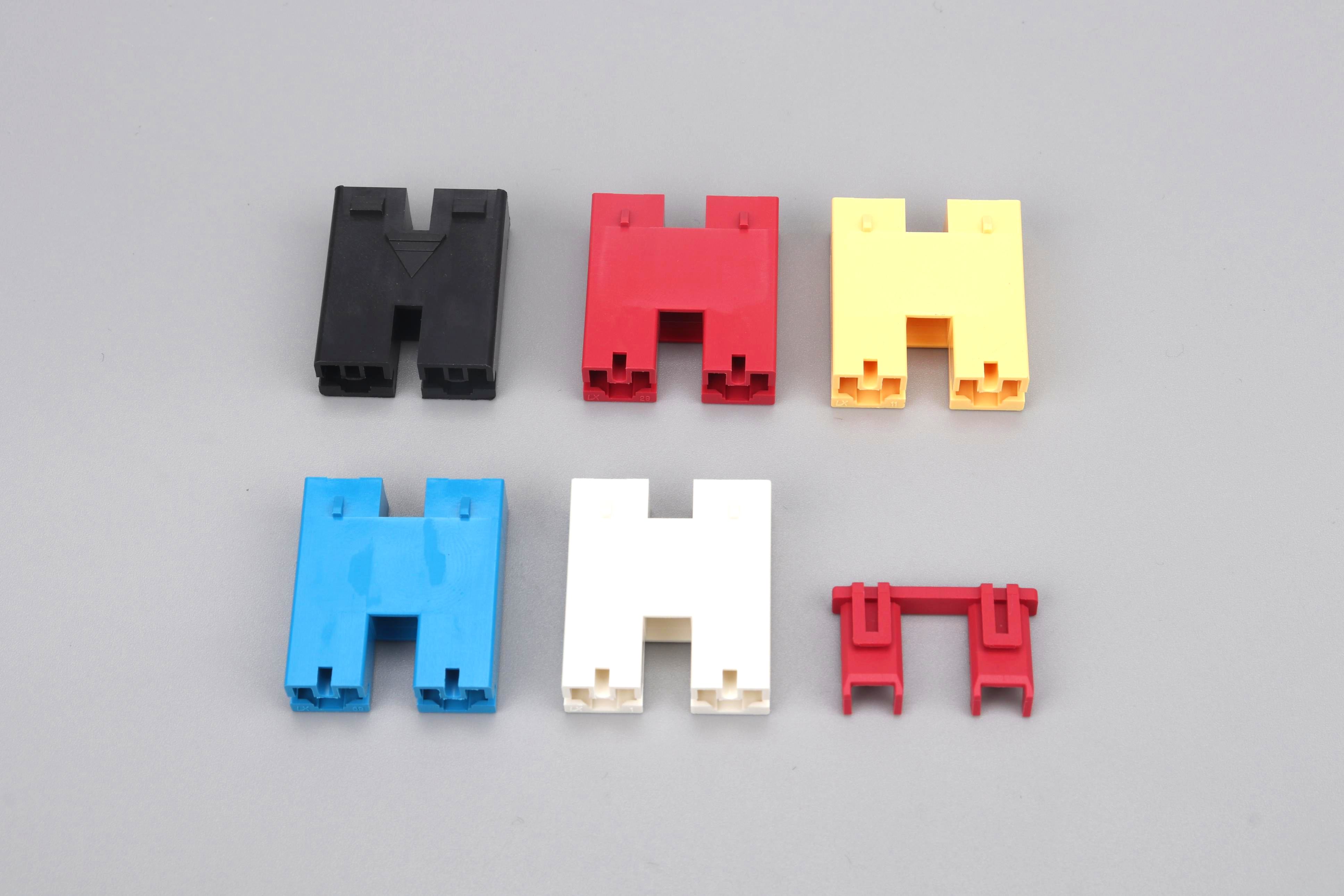
Installing PCB connectors in industrial electronics demands precision, technical knowledge, and adherence to best practices that ensure long-term reliability in demanding operational environments. Whether you are assembling control systems, automation equipment, or ruggedized instrumentation, the quality of your connector installation directly impacts signal integrity, mechanical stability, and overall system performance. Industrial applications impose stricter requirements than consumer electronics, including resistance to vibration, temperature extremes, and electromagnetic interference, making proper installation techniques essential for achieving design specifications and minimizing field failures.
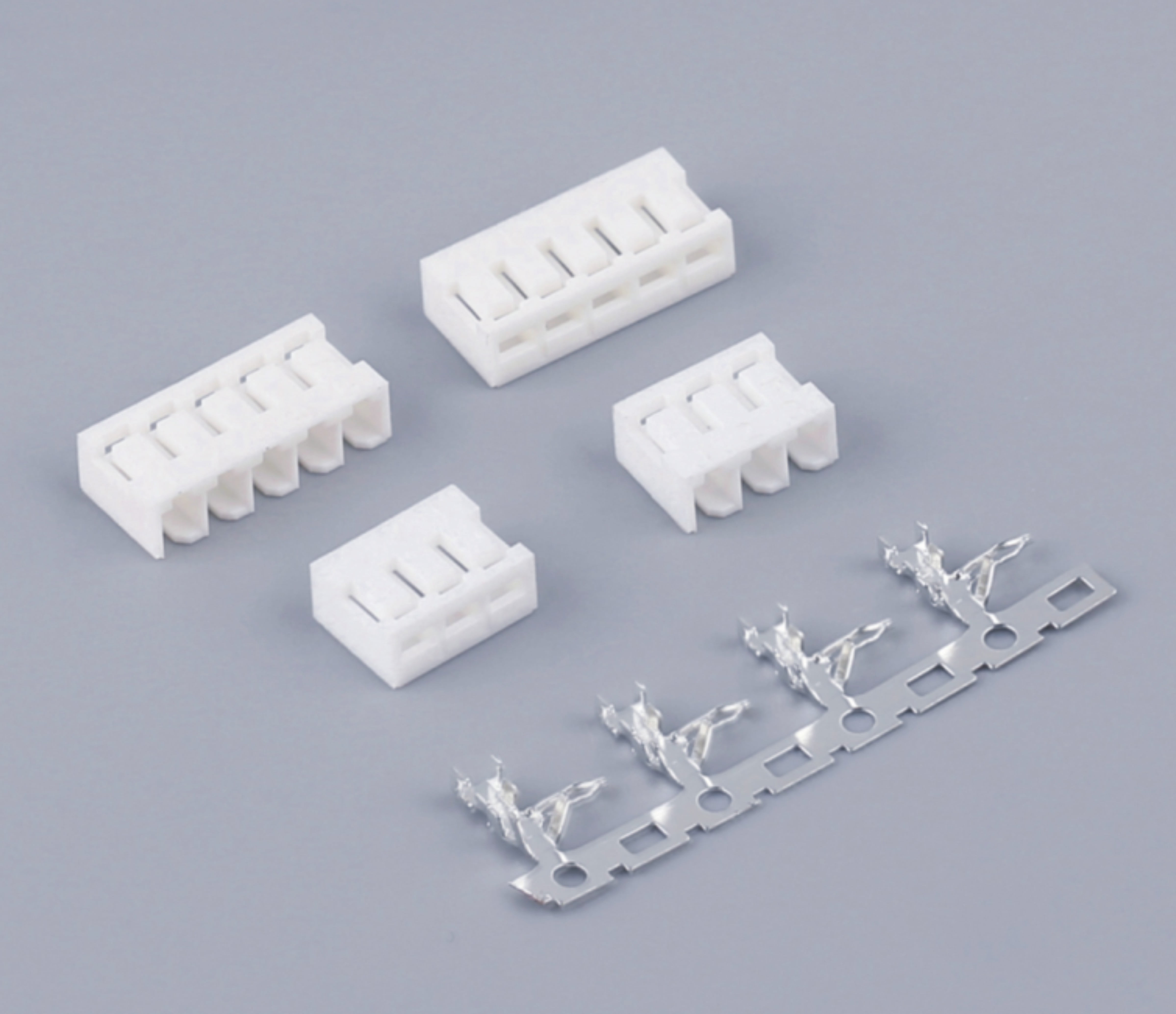
This comprehensive guide provides actionable installation tips for PCB connectors used in industrial electronics, covering preparation, soldering techniques, mechanical considerations, quality verification, and troubleshooting strategies. By following these proven methods, engineers and technicians can achieve reliable connections that withstand the harsh conditions typical of factory floors, outdoor installations, and heavy machinery environments. Understanding the nuances of connector installation helps prevent common issues such as cold solder joints, misalignment, and inadequate strain relief that lead to intermittent failures and costly downtime in industrial settings.
Pre-Installation Preparation and Component Verification
Reviewing Technical Documentation and Specifications
Before beginning any installation work with PCB connectors, thoroughly review all technical documentation provided by the connector manufacturer and the printed circuit board designer. This documentation typically includes pinout diagrams, dimensional tolerances, recommended footprint patterns, and specific installation instructions that address the unique characteristics of each connector family. Industrial-grade PCB connectors often feature specialized mounting requirements or thermal considerations that differ from standard commercial components, making it critical to understand these specifications before proceeding with assembly operations.
Pay particular attention to the connector's pitch specification, mounting style (through-hole versus surface mount), current rating, and voltage rating to ensure compatibility with your application requirements. Verify that the PCB footprint matches the connector's physical dimensions and pin arrangement, as mismatches can lead to installation difficulties or complete incompatibility. For high-reliability industrial applications, also review any derating guidelines that specify reduced current capacity at elevated temperatures or requirements for additional heat dissipation measures when operating in enclosed environments with limited airflow.
Inspecting Components and PCB Quality
Conduct a detailed visual inspection of both the PCB connectors and the printed circuit board before beginning installation work. Examine connector pins for straightness, uniformity, and absence of oxidation or contamination that could compromise electrical contact quality. Industrial environments often expose components to humidity and airborne contaminants during storage, so cleaning connector pins with isopropyl alcohol may be necessary to remove any residues that could interfere with soldering or contact resistance performance.
Inspect the PCB surface for cleanliness, proper solder mask definition around connector pads, and absence of manufacturing defects such as lifted traces or inadequate hole plating. Through-hole PCB connectors require properly sized and plated holes that allow pins to insert smoothly while providing sufficient barrel contact area for reliable solder joints. Surface mount connectors demand flat, coplanar pad surfaces free from solder mask encroachment or contamination that could prevent proper solder wetting during reflow processing.
Organizing Tools and Materials
Assemble all necessary tools and materials before starting connector installation to maintain workflow efficiency and prevent interruptions that could compromise quality. For through-hole PCB connectors, you will need a temperature-controlled soldering station with appropriate tip sizes, rosin-core solder meeting industry specifications, and tools for component positioning and hold-down during soldering. Industrial applications often benefit from dedicated soldering fixtures that secure both the PCB and connector in precise alignment throughout the installation process, particularly when working with multi-row connectors that require simultaneous soldering of numerous pins.
For surface mount PCB connectors, preparation includes solder paste, stencils matched to your specific board design, reflow oven or hot air rework station, and inspection equipment such as magnification systems or automated optical inspection tools. Maintain an organized workspace that minimizes the risk of foreign object contamination, electrostatic discharge damage, or accidental component damage during handling. Having proper ventilation and fume extraction equipment is essential when working with leaded or lead-free solders, as industrial assembly operations often involve extended soldering sessions that could expose personnel to harmful flux vapors without adequate safety measures.
Through-Hole Installation Techniques for Industrial Reliability
Proper Component Insertion and Alignment
When installing through-hole PCB connectors, begin by carefully aligning the connector pins with the corresponding holes in the printed circuit board, ensuring that pin one indicators on both the connector and PCB match according to the assembly documentation. Industrial connectors often feature multiple rows of pins and precise pitch requirements, making alignment critical for successful insertion without bending or damaging pins. Apply gentle, even pressure to seat the connector fully against the board surface, checking that the mounting face makes complete contact with the PCB and that no pins have missed their corresponding holes or become bent during insertion.
For PCB connectors with mounting tabs or additional mechanical anchoring features, verify that these elements properly engage with their designated holes or slots before proceeding with soldering operations. These mechanical features provide essential strain relief in industrial applications where connectors experience repeated mating cycles, vibration exposure, or cable pull forces that could stress solder joints over time. If resistance is encountered during insertion, never force the connector, as this typically indicates misalignment, undersized holes, or pin damage that requires correction before proceeding with installation.
Soldering Parameters and Techniques
Set your soldering iron to the appropriate temperature for the specific solder alloy and PCB connector materials being used, typically between 300°C and 350°C for lead-free solders used in modern industrial electronics. Industrial-grade PCB connectors may incorporate higher-temperature thermoplastics or metal shells that require careful temperature management to prevent damage while achieving proper solder flow and intermetallic formation. Allow the soldering iron tip to heat both the connector pin and the PCB pad simultaneously for one to two seconds before introducing solder, ensuring that heat transfers effectively to create a proper metallurgical bond rather than a cold solder joint that appears acceptable but lacks mechanical strength and electrical conductivity.
Apply sufficient solder to create a smooth fillet that transitions from the pad surface up the connector pin, forming a concave profile that indicates proper wetting and adequate solder volume. Industrial applications demand solder joints that meet IPC-A-610 Class 2 or Class 3 acceptance criteria, depending on the reliability requirements of your specific application. Avoid excessive solder that creates convex joints or bridges between adjacent pins, and never use insufficient solder that leaves gaps or creates weak mechanical bonds vulnerable to failure under vibration or thermal cycling conditions common in industrial environments.
Heat Management and Sequential Soldering
When soldering multi-pin PCB connectors, implement a systematic approach that manages heat distribution across the connector body and prevents cumulative thermal stress that could warp plastic housings or damage internal insulation materials. Begin soldering at diagonal corners to mechanically lock the connector in proper alignment, then proceed with remaining pins in a pattern that allows heat to dissipate between adjacent pin locations. This approach proves particularly important for large connectors with dozens of pins where continuous soldering could elevate the overall connector body temperature beyond material limits.
Monitor the connector housing during soldering operations for any signs of heat distress such as discoloration, softening, or dimensional changes that indicate excessive temperature exposure. Industrial PCB connectors typically specify maximum body temperatures and duration limits that should not be exceeded during assembly operations. If working with thermally sensitive connectors, consider using lower soldering temperatures with longer dwell times, or implement heat sinking techniques that protect the connector body while allowing adequate pin heating for proper solder joint formation.
Surface Mount Installation Best Practices
Solder Paste Application and Stenciling
For surface mount PCB connectors, achieving consistent, high-quality solder joints begins with proper solder paste application using precisely manufactured stencils that match your PCB pad geometry. Industrial applications often require no-clean solder pastes formulated for elevated temperature reflow profiles and extended shelf life in warehouse environments. Select stencil thickness based on the connector pad size and pitch, typically ranging from 100 to 150 micrometers for standard industrial connectors, with thinner stencils used for fine-pitch applications and thicker stencils providing increased solder volume for larger pads that carry higher currents.
Apply solder paste using a consistent squeegee technique that ensures complete aperture filling without excessive paste deposits that could cause bridging between adjacent pads during reflow. Inspect paste deposits after stencil removal to verify proper volume, definition, and absence of smearing or incomplete release from stencil apertures. Environmental control during paste application proves critical for industrial electronics assembly, as temperature and humidity variations can affect paste rheology and printing consistency, potentially compromising solder joint quality for PCB connectors that must perform reliably across extreme operating conditions.
Component Placement Accuracy
Position surface mount PCB connectors onto solder paste deposits with precision that ensures all pads align correctly with their corresponding connector terminations, as misalignment can result in incomplete solder joint formation or electrical opens after reflow processing. Industrial connectors often feature robust mechanical designs with larger body dimensions that provide stable placement characteristics, but their mass also increases the importance of secure adhesion to solder paste before reflow to prevent movement during board handling or oven transport. Use vacuum pickup tools or precision tweezers appropriate for the connector size and weight, avoiding excessive handling that could disturb paste deposits or introduce contamination.
Verify connector orientation according to polarity markings and pin one indicators, as incorrect placement of keyed connectors can render the entire assembly non-functional and require expensive rework operations in industrial production environments. For PCB connectors with fine-pitch terminations or complex pad patterns, consider implementing automated optical inspection or vision-guided placement systems that ensure consistent accuracy across production volumes. Document any placement variations or issues encountered during assembly, as these observations can inform process improvements or design modifications that enhance manufacturability for future production runs.
Reflow Profile Optimization
Develop and validate reflow temperature profiles specifically suited to your PCB connectors and board assembly characteristics, accounting for thermal mass distribution, component heat sensitivity, and solder paste metallurgy requirements. Industrial electronics often incorporate mixed assemblies with both temperature-sensitive components and robust connectors, necessitating careful profile development that satisfies all component requirements simultaneously. Standard lead-free reflow profiles typically include preheat zones reaching 150-180°C, soak zones maintaining temperatures between 180-200°C for 60-90 seconds, and peak reflow zones achieving 240-250°C for 30-60 seconds above liquidus temperature.
Monitor actual board temperatures using thermocouples placed near critical PCB connectors during profile development to ensure that predicted thermal conditions match real-world heating patterns within your specific reflow equipment. Industrial connectors with metal shells or large thermal mass may heat more slowly than smaller components, potentially requiring profile adjustments that extend time above liquidus or increase peak temperatures within allowable limits. After reflow, inspect solder joints for proper fillet formation, complete wetting, and absence of defects such as voids, insufficient solder, or tombstoning that could compromise connector reliability under industrial operating stresses.
Mechanical Considerations and Strain Relief Implementation
Understanding Mechanical Stress in Industrial Applications
Industrial electronics installations subject PCB connectors to mechanical stresses far exceeding those encountered in benign office or residential environments, including constant vibration from machinery operation, shock loads from equipment movement or impact events, and cable pull forces resulting from maintenance activities or thermal expansion of wire harnesses. These mechanical stresses concentrate at the solder joint interface between connector pins and PCB pads, creating fatigue conditions that can eventually lead to crack propagation and electrical failure if not properly addressed through mechanical design and installation practices.
Recognize that PCB connectors serving as board-to-wire interfaces bear the additional responsibility of translating external cable forces into the PCB assembly, making strain relief provisions essential rather than optional for industrial reliability. The interconnection point represents a classic mechanical system combining rigid elements such as connector bodies and circuit boards with flexible elements including solder joints and wire insulation, creating potential failure modes wherever these dissimilar materials interface under stress. Professional installation practices for industrial electronics always incorporate multiple layers of mechanical protection that distribute forces across larger areas and prevent stress concentration at vulnerable solder joints.
Implementing Connector Mounting Hardware
Utilize all mechanical mounting features provided with industrial PCB connectors, including mounting tabs, screw bosses, or board locks that secure the connector to the PCB through means independent of solder joint retention. These mechanical anchoring systems typically provide the primary structural path for forces applied to mated cable assemblies, allowing solder joints to serve their intended electrical function rather than bearing structural loads beyond their design capability. When installing mounting hardware such as screws or standoffs, apply appropriate torque specifications that achieve secure mechanical coupling without over-stressing the PCB substrate or creating compression forces that could crack the board or deform the connector housing.
For PCB connectors without integral mechanical mounting provisions, consider implementing secondary retention methods such as adhesive bonding around the connector perimeter, conformal coating that reinforces solder joint areas, or external brackets that clamp the connector body to the PCB surface. Industrial installations in high-vibration environments may benefit from thread-locking compounds applied to connector mounting screws, preventing gradual loosening that compromises mechanical stability over time. Always verify that mechanical mounting provisions do not interfere with connector mating operations or create accessibility issues for maintenance personnel who must disconnect and reconnect cables during equipment servicing operations.
Cable Management and Strain Relief
Implement proper cable management practices that prevent wire harness weight and movement from transmitting forces directly to PCB connectors, using cable ties, mounting clamps, or strain relief boots positioned at appropriate distances from the connector mating interface. The fundamental principle of strain relief involves anchoring cables to a stable structure before they reach the connector, ensuring that any pulling, bending, or vibration forces dissipate through the cable management system rather than loading the connector and its solder joints. Position the first cable support point within a few centimeters of the connector body, using techniques appropriate for your specific installation including adhesive-backed cable tie mounts, screw-down clamps, or integrated strain relief features built into connector backshells.
In industrial panel mount applications where PCB connectors mate with external cables through enclosure penetrations, coordinate strain relief implementation between internal board-level mounting and external cable gland or connector backshell systems that secure cables to the panel structure. This multi-point approach distributes mechanical loads across several anchoring locations rather than concentrating stress at the PCB interface, significantly improving long-term reliability under the repeated connection cycles and environmental stresses characteristic of industrial field installations. Document cable routing and strain relief configurations in assembly drawings and work instructions to ensure consistent implementation across production units and enable proper maintenance practices that preserve mechanical integrity throughout equipment service life.
Quality Verification and Testing Procedures
Visual Inspection Standards
Conduct systematic visual inspection of all installed PCB connectors using appropriate magnification and lighting to detect potential defects before the assembly proceeds to functional testing or final integration. Industrial quality standards typically reference IPC-A-610 acceptance criteria, which define specific visual characteristics for acceptable solder joints including fillet shape, wetting extent, and allowable defect types based on the reliability class assigned to your product. Examine each solder joint for complete pad coverage, smooth transition from pad to pin, and absence of defects such as insufficient solder, cold joints, bridging between adjacent pins, or contamination that could compromise long-term reliability.
Beyond solder joint quality, verify proper connector orientation, complete seating against the PCB surface, correct alignment of mechanical mounting features, and absence of physical damage to connector housings or pin contacts that could affect mating reliability. For industrial electronics assemblies, visual inspection should also assess the presence and proper implementation of strain relief provisions, cable routing adequacy, and clearance between the installed connector and adjacent components or structures that could create interference during operation or maintenance activities. Document inspection results systematically, using checksheets or digital recording systems that create traceable quality records and enable trend analysis for process improvement initiatives.
Electrical Continuity and Resistance Testing
Perform electrical continuity testing on installed PCB connectors to verify that all intended electrical connections exist and that no unintended shorts or bridges compromise circuit functionality. Use appropriate test equipment such as digital multimeters or automated test systems that can systematically probe each connector pin and verify connectivity to its corresponding PCB trace or component pad. Industrial reliability requirements often demand specific contact resistance limits for connector interfaces, typically below 10 milliohms for power connections and below 50 milliohms for signal paths, necessitating four-wire resistance measurements that eliminate test lead resistance from readings.
When testing PCB connectors that will interface with mating cable assemblies, verify pin-to-pin isolation resistance between non-connected circuits to ensure that no contamination or solder bridges create leakage paths that could cause malfunction under operating conditions. For connectors carrying high-frequency signals, consider implementing time-domain reflectometry or network analyzer measurements that characterize impedance matching and signal integrity parameters critical for reliable data transmission in industrial control networks or instrumentation systems. Document all electrical test results as objective evidence of installation quality, establishing baseline measurements that support future troubleshooting activities if field issues arise during equipment operation.
Mechanical Pull Testing
Implement mechanical pull testing protocols for production qualification or periodic verification that installed PCB connectors meet minimum retention force requirements and that solder joints possess adequate mechanical strength to withstand handling and operational stresses. Destructive pull testing typically involves applying gradually increasing tensile force to the connector body while monitoring for initial movement, crack formation, or complete separation, with acceptance criteria based on connector manufacturer specifications or industry standards for similar component types. Industrial applications may specify pull test requirements ranging from several newtons for small signal connectors to hundreds of newtons for power connectors that must withstand cable pull forces during installation or maintenance operations.
For through-hole PCB connectors, proper solder joint formation typically results in pin fracture or connector housing failure rather than solder joint separation when subjected to pull testing, indicating that the metallurgical bond strength exceeds the connector material strength. Surface mount connectors generally exhibit lower pull strength due to smaller pad areas and absence of mechanical interlocking through PCB holes, making strain relief implementation even more critical for these mounting styles in industrial applications. Conduct pull testing on representative samples rather than every production unit to balance quality verification needs with testing cost and schedule considerations, using statistical sampling plans that provide adequate confidence in installation process capability.
Troubleshooting Common Installation Issues
Addressing Solder Joint Defects
When encountering solder joint defects on installed PCB connectors, first identify the specific defect type through visual inspection or electrical testing, as different defect mechanisms require different corrective approaches. Cold solder joints appearing dull and grainy typically result from insufficient heat during soldering, contaminated surfaces that prevent proper wetting, or component movement during solder solidification. Rework cold joints by applying additional heat and fresh solder after thoroughly cleaning the affected area, ensuring that both the connector pin and PCB pad reach proper soldering temperature before introducing new solder material.
Insufficient solder deposits that fail to create proper fillets or leave gaps in pad coverage usually indicate inadequate solder application during initial assembly, requiring solder addition while carefully managing heat input to avoid damaging the connector or adjacent components. Conversely, excessive solder creating bridging between adjacent pins necessitates removal techniques using desoldering braid or vacuum desoldering equipment, followed by careful inspection to verify that pad surfaces remain intact and suitable for re-soldering. Industrial rework operations on PCB connectors must maintain the same quality standards applied during initial assembly, using calibrated equipment and trained personnel to ensure that reworked connections achieve full design reliability rather than representing weak points vulnerable to premature failure.
Resolving Alignment and Fit Problems
Address PCB connectors that fail to insert properly or exhibit alignment difficulties by first verifying that the correct connector part number matches the specified component for your board design, as similar-appearing connectors may have subtle dimensional differences that prevent proper installation. Examine connector pins for straightness using a magnifying glass or microscope, as bent pins often result from handling damage or previous insertion attempts and may require careful straightening with precision tools before successful installation becomes possible. For through-hole connectors, verify that PCB hole sizes meet design specifications and that holes are properly plated without obstruction from solder mask or manufacturing residues that could prevent pin insertion.
When PCB connectors exhibit excessive play or fail to seat completely against the board surface, investigate potential causes including warped PCBs, dimensional tolerance stack-up issues, or connector manufacturing variations that fall outside acceptable limits. Industrial electronics assemblies may require shim adjustments or localized board flattening techniques to achieve proper connector seating, particularly for large multi-row connectors spanning significant board areas where slight warpage can prevent uniform contact. Document any fit issues encountered during installation and communicate findings to design engineering teams, as persistent problems may indicate design modifications needed to improve manufacturability or component specification changes required to ensure consistent assembly quality across production volumes.
Correcting Post-Installation Failures
When installed PCB connectors fail during functional testing or exhibit intermittent behavior, conduct systematic troubleshooting that isolates the failure mechanism and identifies appropriate corrective actions. Electrical opens typically result from incomplete solder joint formation, cracked solder connections, or internal connector contact failures that may not be visible through external inspection. Use electrical probing techniques to verify connectivity at multiple points along the signal path from PCB pad through connector pin to mating interface, identifying where continuity breaks occur and whether failures reside in solder joints, connector bodies, or mating cable assemblies.
Intermittent connections that appear during vibration or temperature cycling often indicate marginal solder joints with partial wetting, cold joint characteristics, or inadequate mechanical support that allows micro-movement under stress. These challenging defects may require thermal cycling testing or vibration exposure to reproduce failure conditions reliably, enabling observation of failure mechanisms under controlled conditions that guide rework strategies. For PCB connectors in industrial electronics, never accept intermittent failures as acceptable quirks requiring workarounds, as these symptoms invariably indicate underlying quality issues that will worsen over time and lead to complete failure under field operating conditions. Implement thorough root cause analysis for any installation-related failures, using findings to refine processes and prevent recurrence rather than simply reworking affected units without understanding failure mechanisms.
FAQ
What solder temperature should I use for industrial PCB connectors?
For industrial PCB connectors, use soldering iron temperatures between 300°C and 350°C when working with lead-free solder alloys, adjusting based on connector thermal mass and heat sensitivity. Larger connectors with substantial metal shells may require temperatures at the higher end of this range to achieve adequate heat transfer, while smaller connectors or those with temperature-sensitive plastic housings benefit from lower temperatures with slightly longer dwell times. Always verify that your selected temperature falls within the connector manufacturer's specified limits and produces proper solder flow with smooth, shiny joints indicating complete metallurgical bonding. For reflow soldering of surface mount connectors, develop profiles that achieve peak temperatures of 240-250°C for 30-60 seconds above liquidus, ensuring adequate thermal soak periods that prevent thermal shock while achieving complete solder reflow.
How can I prevent solder bridges between closely spaced connector pins?
Prevent solder bridges on fine-pitch PCB connectors by using appropriately sized soldering iron tips that deliver heat precisely to individual pins without excessive thermal spread to adjacent locations, typically choosing chisel or conical tips with widths smaller than the pin spacing. Apply solder sparingly, building proper fillet geometry gradually rather than depositing excessive amounts that flow between pins during the molten phase. Maintain clean, tinned soldering iron tips that promote efficient heat transfer and allow solder to flow onto intended surfaces rather than clinging to oxidized tip surfaces. For surface mount connectors prone to bridging, optimize solder paste stencil aperture designs that deposit appropriate solder volumes matched to pad sizes, and ensure proper reflow profile development that allows controlled solder wetting without excessive flow. When bridges do occur, remove them promptly using desoldering braid or vacuum desoldering techniques before solder fully solidifies.
What mechanical retention force should PCB connector solder joints withstand?
Industrial PCB connector solder joints should withstand mechanical pull forces specified by the connector manufacturer, typically ranging from 10-50 newtons for small signal connectors to 100-500 newtons for larger power connectors, depending on pin count, mounting style, and intended application severity. Through-hole mounted connectors generally provide higher retention strength than surface mount types due to mechanical interlocking through plated holes in addition to solder bond strength. However, proper installation practices dictate that mechanical loads should not rely solely on solder joint strength regardless of measured pull test values. Instead, implement dedicated mechanical mounting provisions such as screws, board locks, or mounting tabs that create structural load paths independent of solder connections, allowing electrical joints to serve their primary purpose without bearing sustained mechanical stress that accelerates fatigue failure under vibration or thermal cycling conditions typical of industrial environments.
How do I verify that a connector is properly seated before soldering?
Verify proper connector seating by inspecting the mounting face for complete, uniform contact with the PCB surface across the entire connector footprint, checking for gaps or raised areas that indicate incomplete insertion or interference from underlying components. For through-hole PCB connectors, examine pin protrusion on the solder side of the board to confirm that all pins extend approximately equal distances beyond pad surfaces, indicating that no pins have missed their holes or failed to insert completely. Gently press on the connector body to confirm solid contact without perceivable movement or springback that would suggest incomplete seating or interference. Use backlighting or side viewing angles that reveal gaps between connector mounting surfaces and PCB that may not be visible from directly above. For connectors with positive latching features such as board locks or snap-in tabs, verify audible or tactile confirmation of engagement before proceeding with soldering operations, as these mechanical indicators provide definitive evidence of correct installation position.
Table of Contents
- Pre-Installation Preparation and Component Verification
- Through-Hole Installation Techniques for Industrial Reliability
- Surface Mount Installation Best Practices
- Mechanical Considerations and Strain Relief Implementation
- Quality Verification and Testing Procedures
- Troubleshooting Common Installation Issues
- FAQ

